絶縁ゲート ドライバー

安定化バイポーラ出力対応のセルフパワー絶縁型GaN FETドライバ

AHV85111

AHV85111は、GaN FET向けに高精度の柔軟なゲート ドライブを提供します。安定化されたバイポーラ出力、調整可能な正電圧レール、内蔵のバイアス電源により、設計を簡素化してdv/dt耐性を向上させます。

Product Details

Top Features

  • Transformer isolation barrier
  • Power-Thru integrated isolated bias
    • No need for high-side bootstrap
    • No need for external secondary-side bias  
  • AEC-Q100 Grade 2 qualification
  • Bipolar drive output with adjustable regulated positive rail
  • Built-in primary-side 3.3V REF bias output
  • 50ns propagation delay
  • Separate drive output pins: pull-up (2.8 Ω) and pull-down (1.0 Ω)
  • Supply voltage 10.8 V < VDRV < 13.2 V
  • Undervoltage lockout on primary VDRV and secondary VSEC
  • Enable pin with fast response
  • Continuous ON capability—no need to recycle IN or recharge bootstrap capacitor
  • CMTI > 100 V/ns dv/dt immunity
  • Creepage distance 8.4 mm
  • Safety Regulatory Approvals
    • 5 kV RMS VISO per UL 1577
    • 8 kV pk VIOTM maximum transient isolation voltage
    • 1 kV pk maximum working isolation voltage

Part Number Specifications and Availability

Part Number Specifications and Availability

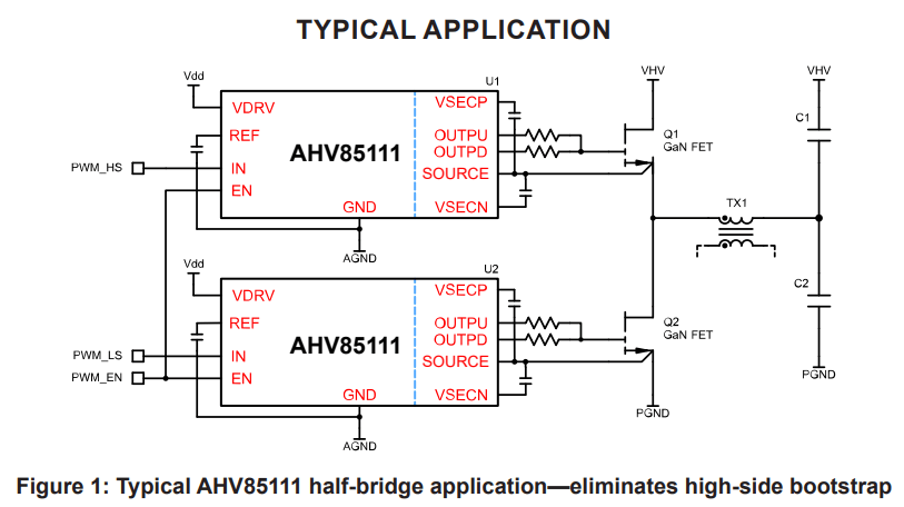
AHV85111 Product Overview

The AHV85111 isolated gate driver is optimized for driving GaN FETs in multiple applications. An isolated dual positive/negative output bias supply is integrated into the driver device, eliminating external gate drive auxiliary bias supply or high-side bootstrap.

設計ツール