An Efficient Voltage Optimized LED Driver (A80804) With Synchronous Buck Pre-Regulator Module (APM81911)
Introduction
Linear LED drivers dissipate significant power proportional to difference in input and output voltage. Due to such excessive power dissipation, linear LED drivers are used at lower currents and need bigger power packages and larger PCB size, or heat sinks to maintain the temperature within desired specification. For solving such issues, a pre-regulator is generally used to feed linear drivers which efficiently reduce output voltage to lower levels for better power efficiency, and eventually better thermal performance. However, due to variation in LED forward voltage tolerance and active switching of series connected LEDs, the output voltage of the pre-regulator needs to be designed for the highest voltage, which results in significant power loss at lower LED voltage.
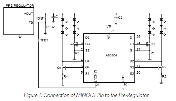
This application note presents the implementation of adaptive pre-regulator where output voltage is dynamically adjusted to provide optimum voltage to the LED driver. The front-end buck regulator module (APM81911) provides supply voltage to the linear LED controller (A80804) which controls the LED current. To achieve better efficiency, the LED controller (A80804) controls the output voltage of the pre-regulator to minimum voltage required for LED regulation. This is implemented with the MINOUT pin in the A80804, which provides an output voltage proportional to the minimum voltage of the drain pins of all the active channels. The voltage from MINOUT can be fed to a voltage regulator’s feedback pin to complete the closed-loop system and trim the regulated output voltage fed to the LEDs.
Figure 1 shows the connection of the MINOUT pin of the A80804 which provides feedback to the pre-regulator for optimal voltage control.
Device Overview
This section presents the overview of the APM81911 and A80804 device.
A80804 LED Driver
The A80804 is linear, programmable current controller capable of accurately regulating current in four LED strings using external MOSFETs. Each of the four LED drivers has an independent enable/PWM input and current-sense resistors. Each channel can be independently dimmed with an external PWM signal, or all channels can be dimmed with internal PWM dimming and automatic phase shifting. The overall LED current can be switched between low and full intensity for applications including stop/tail or DRL/position lighting.
Multiple analog-dimming options are available to support applications including LED binning, NTC foldback, or hybrid dimming. A selectable LED current slew-rate control is available to tune PWM edge times and improve EMI performance. The A80804 also offers several fault detection and protection required for Automotive applications. The A80804 can be configured for either one-out-all-out or N-1 operation.
APM81911 Buck Module
The APM81911 is a highly integrated synchronous DC-DC regulator module rated for 3 A. It includes a DC-DC regulator, low DCR inductor and two capacitors in a compact 4 mm × 6 mm × 2 mm package. The APM81911 offers scalable output with ±1.5% output voltage accuracy over the full operating temperature.
Fixed frequency, peak current mode ensures rapid response to load and line transients. Spread spectrum operation is used for lower EMI/EMC. The APM81911 can be synchronized to an external clock.
Low power (LP) mode maintains the output voltage at no load or very light load conditions while drawing < 6 uA. The APM81911 automatically transitions to PWM and LP modes depending on load current.
The APM81911 includes adjustable soft start and an open-drain power good output; the module additionally includes accurate enable input programmable turn-on and turn-off thresholds, and a low shutdown current of 1 uA.
System Specification
This section shows the key system specifications and the calculation of bias resistors for implementation of the MINOUT feature.
The input voltage specification of the system, key buck regulator specifications, and LED specifications are given below:
□ Nominal Input Voltage (VIN,NOM) = 12 V
□ Minimum Input Voltage (VIN,MIN) = 8 V
□ Maximum Input Voltage (VIN,MAX) = 18 V
The Key Buck Regulator Specifications are as follows:
□ Operating Frequency (fSW) = 2.1 MHz
□ Output Capacitor (COUT) = 33 μF
□ Regulator Feedback Voltage (VFB) = 800 mV
The key LED specifications are as follows:
□ LED Typical Forward Voltage (VF,TYP) = 3.1 V
□ LED Max. VF (VF,MAX) = 3.3 V
□ LED Min. VF (VF,MIN) = 2.8 V
□ LED Current = 300 mA
The following are the system specifications, pertaining to the margins required in the calculation of the minimum and maximum output voltage:
□ Regulation Voltage Drop on Sense Resistor (VSENSE) = 500 mV
□ MOSFET Voltage Drop (VMOS) = 200 mV
□ Maximum Margin for transient and regulator tolerance (VMARGIN,MAX) = 0.7 V
□ Minimum Margin for transient and regulator tolerance (VMARGIN,MIN) = 0.3 V
Based on the above specifications, the maximum and minimum output voltage can be calculated as shown below.
□ Maximum Output Voltage (VOUT,MAX):
VOUT,MAX = VfMAX + VSENSE + VMOS + VMARGIN,MAX
VOUT,MAX = 3.3 + 0.5 + 0.2 + 0.7 = 4.7 V
□ MinimOutput Voltage (VOUT,MIN):
VOUT,MIN = VfMAX + VSENSE + VMOS + VMARGIN,MAX
VOUT,MAX = 2.8 + 0.5 + 0.2 + 0.3 = 3.8 V
Now the resistors connected on the MINOUT pin as shown in figure 1, can be calculated as below.
□ Selecting RFB2 = 10 kΩ
□ Calculate RFB1 and RFB3 using the below formulas:

□ Maximum MINOUT Voltage (VMINOUT,MAX) = 3.5 V
□ Using above formulas, the value of RFB3 and RFB1 are calculated as,
♦ RFB3 = 179 kΩ (Selected value as 165 kΩ, 1%)
♦ RFB1 = 46 kΩ (Selected value as 47 kΩ, 1%)
Operation
A typical application with a linear LED driver with pre-regulator is shown in Figure 1. The A80804 regulates the LED current. The voltage on the Dx pins is the difference between pre-regulator output voltage and LED forward voltage drop. The A80804 needs a minimum 0.5 V on Dx pin for accurate LED current regulation, but any additional voltage on these pins results in extra power loss in the external MOSFETs.
As shown in figure 2, the MINOUT pin provides an output voltage proportional to the minimum voltage of the Dx pins for all active channels. The voltage from MINOUT is fed to a voltage regulator’s FB pin to complete a closed-loop system and trim the regulated output required to driver LEDs. The voltage on MINOUT is shown in the following equation:
VMINOUT = 10 × (VDxMIN – 0.8) + 0.3
The MINOUT pin has range of 0.3 to 3.5 V.
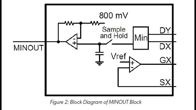
It is important to note that if the LED strings’ voltages change due to temperature change or active switching of number of LEDs, the MINOUT voltage changes and provides proper feedback signal to the pre-regulator to adjust output voltage to optimum level.
Test Results
This section presents the steady state, transient, and stability performance of the overall system.
Steady-State Performance
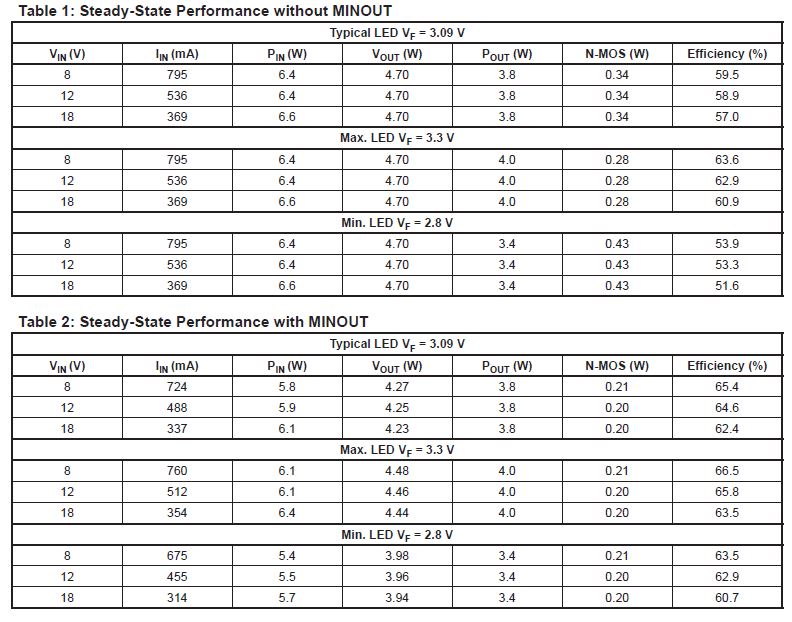
Figures 3 (A), (B), (C) and 4 (A), (B), (C) show the operation of the LED driver without and with MINOUT feature at supply voltage of 8, 12, and 18 V respectively.

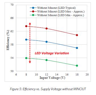
Power Efficiency
Table 1 and Table 2 show the steady state performance of the system without and with MINOUT feature respectively. Moreover, Fig. 5 and 6 show the plot of efficiency vs input voltage of the system without and with MINOUT respectively. As shown in these figures, the efficiency of the system implemented with MINOUT feature is higher as compared to system without MINOUT implementation. The efficiency difference becomes higher as the LED voltage drops as shown in these figures.

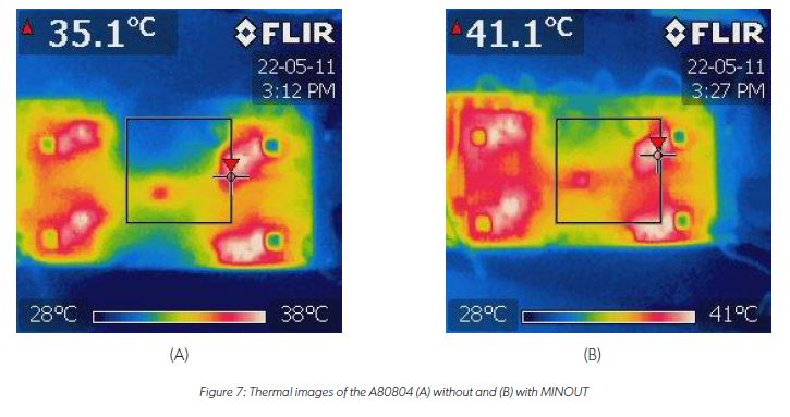
Thermals
Figure 7 (A) and figure 7 (B) show the thermal images of the A80804 board without and with MINOUT, respectively. As the images illustrate, a better thermal outcome is acheived with MINOUT.
Stability
Figures 8 and 9 show the bode plot depicting sufficient gain and phase margins without and with MINOUT, respectively. The stability of the overall system is primarily set by the pre-regulator compensation loop, and is not affected by the LED driver. The MINOUT finction is notably slow, and does not impact overall frequency response.


Load Current Transients - Sequential Operation
In sequential LED driver application, same number of LEDs are sequentially turned on. The output voltage remains almost constant, however the overall input current changes with the number of LED turning on and off. The voltage of the MINOUT pin also does not change significantly as output voltage remains almost constant.
Figure 10 shows the sequential operation of the system at the rated input voltage of 12 V.

Load Current Transients - Single LED Operation
In single LED operation, the sense resistor of the LED is changed dynamically to check the system performance. Figure 11 shows the single LED operation with current changing from 1.2 to 1.6 A with output voltage remaining constant.

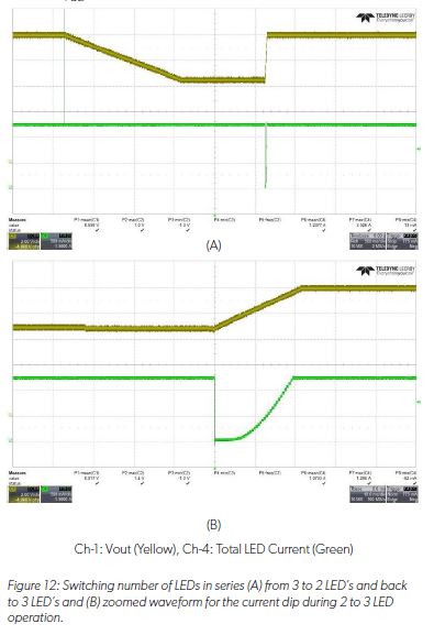
Load Voltage Transients (Tail/Stop or DRL/POS)
In Tail/Stop or DRL/POS applications, usually few numbers of LEDs are switched on and off, which changes the output voltage of the pre-regulator. The MINOUT function adjust the output voltage of pre-regulator to desired level to achieve best efficiency.
Figure 12 (A) shows typical operation when number of LEDs switched from 3 LEDs to 2 LEDs and back to 3 LEDs. LED current is set to 300 mA per channel. When 3 LEDs switched to 2 LEDs, output voltage of pre-regulator drops slowly without causing any disturbance in LED current. However, when 2 LEDs switched to 3 LEDs, suddenly output voltage required to increase, which can result in a glitch in LED current due to limited response of MINOUT.
The values of various feedback resistors used for this test are as follows:
♦RFB1 = 117 kΩ
♦RFB3 = 86.6 kΩ
♦RFB2 = 10 kΩ
Application Simplified Schematics
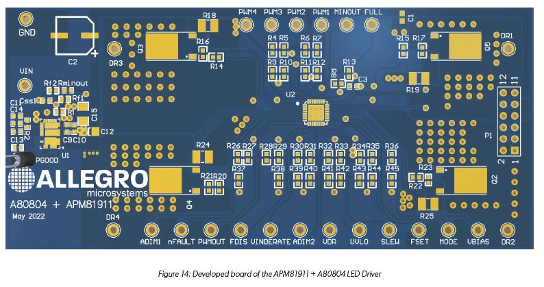
Figure 13 shows the application schematics of the LED driver with a front end APM81911 Buck Converter and an A80804 LED controller. Figure 14 shows the developed two-layer board without components. The overall board dimensions are 4.6 in × 2.1 in.

Layout
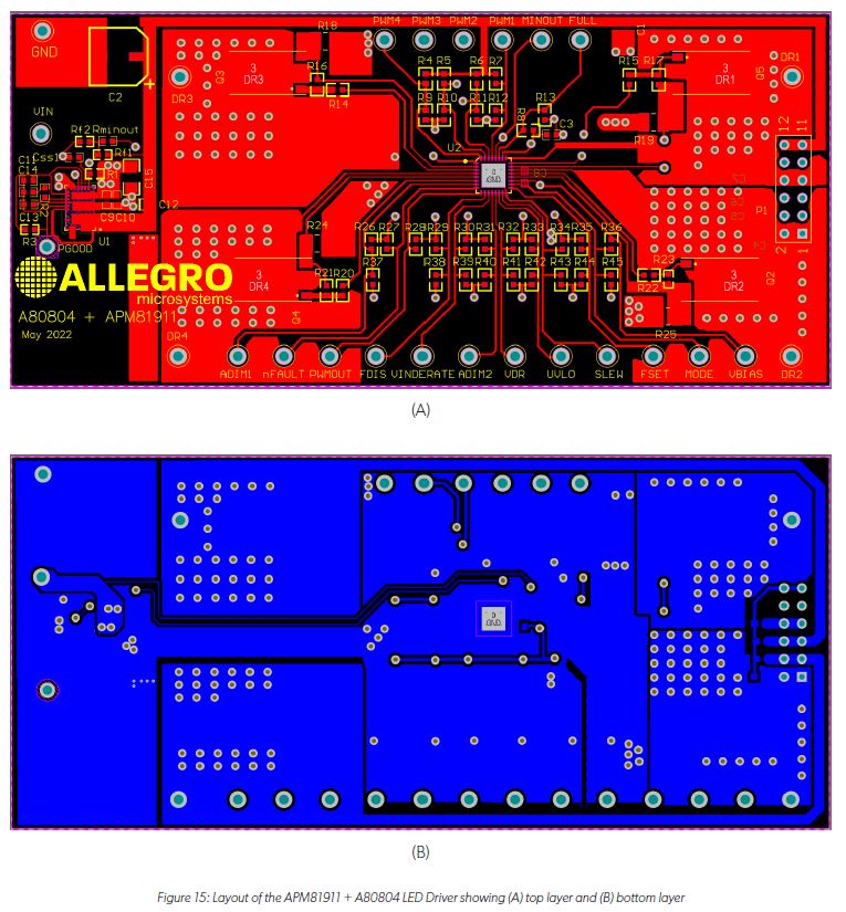
Figure 15 shows the layout (top layer and bottom layer) of the developed LED driver with a front end APM81911 and an A80804 LED controller.
Bill of Materials

Pin Configurations
APM81911
EN/UV: Connected to VIN to enable device.
FSET: Connected to VCC for default 2.15 MHz switching frequency.
PWM/AUTO: Connected to GND for AUTO transition between PWM and PFM modes.
A80804
SLEW: Connected to VBIAS for 80 µS slew time.
ADIM1, ADIM2: Connected to VBIAS to disable analog dimming.
VINDERATE: Connected to VBIAS to disable input voltage derating. VIN pin is connected to input battery supply and LEDs are connected to different voltage. In this case, VINDERATE will not work.
FSET: Driver works in full mode, so PWM mode does not matter.
FDIS: Disable FDIS by connecting to VBIAS.
MODE: Connect to low for N-1 fault operation.
UVLO: Disable UVLO by connecting to GND.
VDR: Sets PWM duty in internal PWM mode. As the driver is configured in FULL mode, VDR pin voltage does not matter.
Conclusion
This application note presents a high efficiency sequential LED driver using Allegro MicroSystems’ APM81911 + A80804 devices. The high efficiency is achieved by optimally controlling the output of a switching buck pre-regulator.
A design procedure for the selection of the components has been presented. An efficiency comparison of the system with and without MINOUT feature has been shown and a significant increase in efficiency has been reported. The steady-state waveforms have been presented for full-load (all 4 LEDs operating at 300 mA each) at the supply voltages of 8, 12, and 18 V with and without the MINOUT feature implementation. The device stability has also been verified over wide range of input voltages.
Copyright 2022, Allegro MicroSystems.
The information contained in this document does not constitute any representation, warranty, assurance, guaranty, or inducement by Allegro to the customer with respect to the subject matter of this document. The information being provided does not guarantee that a process based on this information will be reliable, or that Allegro has explored all of the possible failure modes. It is the customer’s responsibility to do sufficient qualification testing of the final product to ensure that it is reliable and meets all design requirements.
Copies of this document are considered uncontrolled documents.