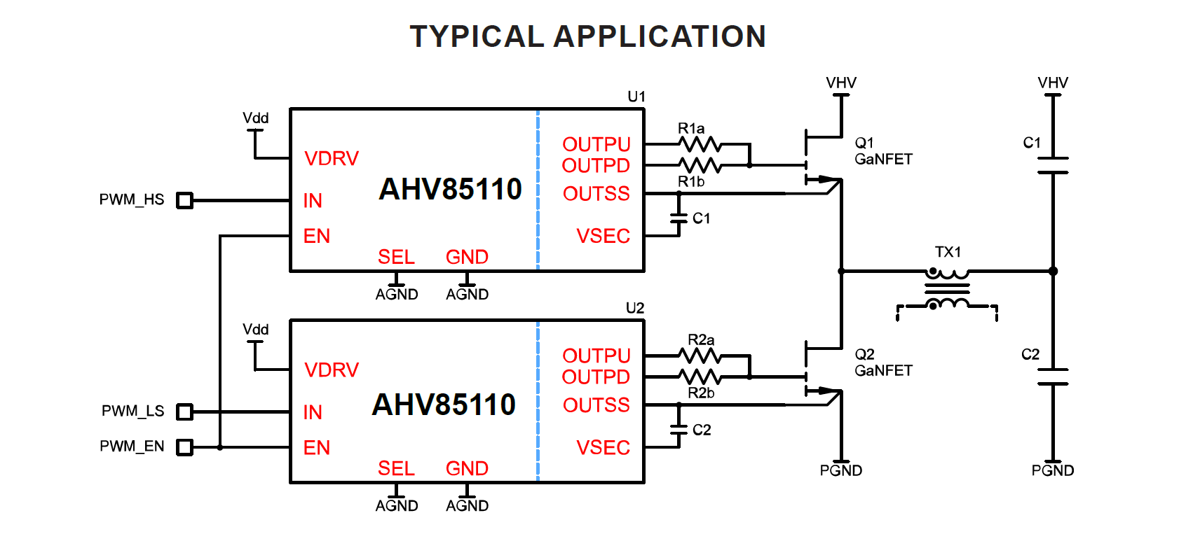
AHV85110简化了GaN FET隔离栅极驱动设计,并集成偏置电源,无需外部元件。它具有高 dv/dt 抗扰度、快速传播延迟和强大的保护功能。
Product Details
Product Details
Top Features
- Transformer isolation barrier
- Power-Thru integrated isolated bias
- No need for high-side bootstrap
- No need for external secondary-side bias
- AEC-Q100 Grade 2 qualification
- 50 ns propagation delay
- Separate drive output pins: pull-up (2.8 Ω) and pull-down (1.0 Ω)
- Supply voltage 10.5 V < VDRV < 13.2 V
- Undervoltage lockout on primary VDRV and secondary VSEC
- Enable pin with fast response
- Continuous ON capability—no need to recycle IN or recharge bootstrap capacitor
- CMTI > 100 V/ns dv/dt immunity
- Creepage distance 8.4 mm
- Safety Regulatory Approvals
- 5 kV RMS VISO per UL 1577
- 8 kV pk VIOTM maximum transient isolation voltage
- 1 kV pk maximum working isolation voltage
Target Application
- DC-DC Converter
- Auxilary Inverter
- On-board Charger
- Server Power
- C&I Solar String Inverters

Part Number Specifications and Availability
HV Isolated Evaluation Boards
| EVK PN | Switch | Supplier / PN | Description | Gate Driver Used | |
|---|---|---|---|---|---|
| APEK85110KNH-01-T-MH Evaluation Board User Guide (GaN Systems FETs) | E-Mode GaN | GaN Systems GS66516B | Half-bridge bipolar driver-switch board | AHV85110 | Buy Now |
| APEK85110KNH-05-T-MH Evaluation Board User Guide (Nexperia FETs) | E-Mode GaN | Nexperia GAN080-650EBE | Half-bridge bipolar driver-switch board | AHV85110 | Buy Now |
| APEK85110KNH-06-T Evaluation Board User Guide (Transphorm FETs) | GaN | Transphorm TP65H070G4QS | Half-bridge bipolar driver-switch board | AHV85110 | Buy Now |
AHV85110 Product Video
The AHV85110 isolated gate driver is optimized for driving GaNFETs in multiple applications and topologies. An isolated output bias supply is integrated into the driver device, eliminating the need for any external gate drive auxiliary bias supply or high-side bootstrap. This greatly simplifies the system design and reduces EMI through reduced total common-mode (CM) capacitance. It also allows the driving of a floating switch in any location in a switching power topology.
0:00

Technical Documentation

Application Note
Minimizing PCB Parasitic Effects with Optimum Layout of the Gate Driver Loop Applicable to AHV85110 AND AHV85111 Gate Drivers
Application Note
Design and Application Guide for AHV85110
Application Note
FET Gate Drive and Bipolar Output Applicable to AHV85110KNHTR Gate Drivers
Blog
Powering the Next Generation of High-Density GaN Modules: Allegro MicroSystems + RAM Innovations New

Brochure
Robust and Efficient UPS Solutions Powered by Allegro
Brochure
Brochure: The AHV85110 Overview
Brochure
Precision in Motion: Powering the Future of Collaborative Robotics
Brochure
Empowering the Renewable Grid - Driving Efficiency, Reliability, and Density in Solar String Inverters
Brochure
Robust and Efficient Power Supply Units (PSUs) for Cloud Infrastructure
Brochure
太阳能收集
Brochure
电动汽车热管理系统
Brochure
DC 快速充电:速度更快、行程更远
Brochure
通过可持续性实现舒适性

Guide
AHV85110 Simplis Modeling Guide
Guide
APEK85110KNH-06-T Evaluation Board User Guide (Transphorm FETs)
Guide
APEK85110KNH-01-T-MH Evaluation Board User Guide (GaN Systems FETs)
Guide
APEK85110KNH-05-T-MH Evaluation Board User Guide (Nexperia FETs)

Infographic
Power-Thru-Technology Infographic

Technical Article
Solving the Challenges of Increasing Power Density by Reducing Number of Power Rails
Technical Article
Simplify Designs and Reduce Overall Systems Cost by Eliminating External Power Supplies
Technical Article